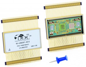
MIL-STD-1553 components are available in a variety of packages. The selection of a component depends on many factors. The enviorment that the component is used in has a very large influence on your selection.
Components are made from different substances, in order to function is particular environments. They come on many sizes, and contain different aspects of MIL-STD-1553.
Packages
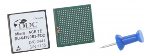
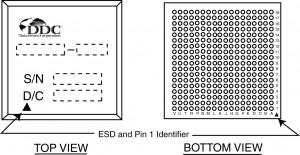
BGA
A Ball Grid Array (BGA) is a surface-mount package used for integrated circuits. A BGA is a package with one face covered, or partly covered, with solder balls in a grid pattern. The package is placed on a PCB with copper pades in a patten that matches the solder balls. The assembly is heated, which causes the solder balls to melt, and then the solder cools and solidifies, holding the package to the PCB.
| Advantages | Disadvantages |
|---|---|
| High Density – a solution to the problem of producing a miniature package for an integrated circuit with hundreds of pins. As package pins got closer, the danger or accidentally bridging adjacent pins with solder grew. BGAs do not have this problem when the solder is factory-applied to the package. | Noncompliant Leads – Solder balls cannot flex (non-compliant) in the way that longer leads can. As with all surface mount devices, bending, due to a difference in coefficient of thermal expansion between PCB substrate and BGA (thermal stress), or flexing and vibration (mechanical stgress) can cause the solder joints to fracture. |
| Heat Conduction – BGA packages have lower thermal resistance between the package and the PCB, than discrete lead packages. The BGA allows heat generated by the integrated circuit inside the package to flow more easily to the PCB, preventing the chip from overheating. | Inspection – once a BGA package is soldered down, it may be difficult to look for soldering faults. X-ray machines, Industrial CT Scanning machines, special microscopes,a nd Boundary Scan testing have been developed to inspect soldering.. |
| Low-Inductance Leads – the shorter an electical conductor, the lower its inductance, a property which causes an unwanted distortion of signals in high-speed electronic circuits. BGAs, with their very short distance between the package and the PCB, have low inductances and therefore have far superior electrical performance to leaded devices. | Sockets – sockets for BGAs, often needed during development, tend to be unreliable. There are two common types of socket. The more reliable type has spring pin that push up under the balls. The less reliableis a ZIF socket, with spring pinchers that grab the balls. |
| Expensive Equipment Required – expensive equipment is required to reliably solder BGA packages. Soldering BGA packages by hand is very difficult and unreliable. |
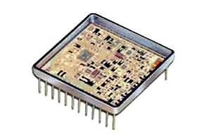
DIP
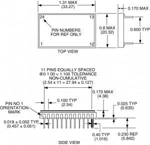
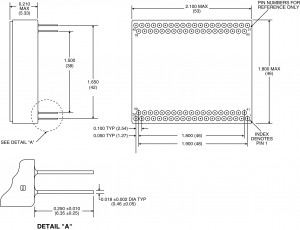
A Dual In-Line Package (DIP) is an electronic device package with a rectangular housing and two parallel rows of electrical pins. The pins are all parallel, point downward, and extend past the bottom plane of the package at least enought to be through-hole mounted to a PCB.
DIP packages are the most popular first generation IC package type. The typical lead spacing of the package is 0.100″ on two sides of the package body. The body width varies: 0.300″, 0.400″, 0.600″, and 0.900″.
| Advantages | Disadvantages |
|---|---|
| Board Space – no extra board space is needed, since the leads are directly underneath the package. | Expense– additional drilling is required to use DIP packages, which makes the boards more expensive to produce. |
| Strength – soldering the DIP via through-hole solder provides a much stronger bond than a surface-mount solder . | Limitations – DIP packages limit the available routing area for signal traces on layers immediately below the top layer on multilayer boards, since the holes must pass through all layers of the to the opposite side. |
| Mounting Options – DIP packages can be mounted to a PCB in two ways. One is through-hole solder. The other is am inexpensive spring-contact sockets. |
Flat Pack
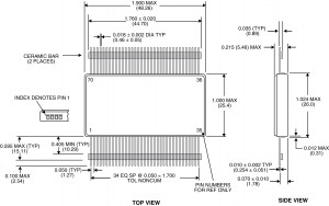
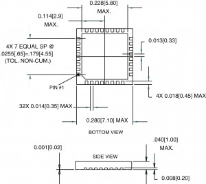
A Flat Pack is a US military standardized printed circuit board surface mount component package. It is a rectangular or square package with leads parallel to base plane attached on two opposing sides of the package periphery. Quad Flat Packs have leads on all four sides of the package.
Flat packs, that have leads extending from only two sides of their body, are only available with 50 mil (1.27 mm) lead pitch. Therefore, they have a low lead count such as 14, 16, or 28 leads, though some large packages can have up to 80 leads.
Quad flat packs, which have leads on all four sides of the package, are available with a lead pitch of 25.6 (.65 mm) down to 11.8 mils (.3 mm). Lead counts as high as 304 leads are available.
| Advantages | Disadvantages |
|---|---|
| Reliability – flat packs are the oldest surface mount IC package, developed in 1962. | Storage– the flat leads on the flat pack must be stored in special carriers, to prevent lead damage. |
| Applications – flat packs are only used for MIL Spec and aerospace, so they are designed for the inteded use of MIL-STD-1553. | Lead Forming – just prior to use, the flat leads are cut and bent into gull-wings by using lead forming equipment. Lead forming equipment in an extra expense. Since leads are usually gold, they must be pre-tinned prior to assembly. |
Gull Wing
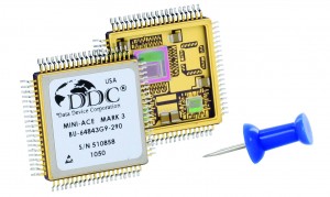
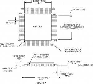
The gull wing package leads are formed in a profile very similar to the outline of a seagull’s wings. The gull wing is considered one of the most reliable terminations for fine-pitch high pin-count packages.
Such as the quad flat packs, gull wing packages are available with a lead pitch of 25.6 (.65 mm) down to 11.8 mils (.3 mm). Lead counts as high as 304 leads are available. These leads are individually soldered to the PCB.
| Advantages | Disadvantages |
|---|---|
| Inspection – gull wing packages allows easy inspection of the solder connections between the lead and the board. | Board Space– the gull wing takes up more board space because leads are to the outside of the chip body. |
| Storage – the gull wing packages are stored in standard trays. |
LPCC
A Leadless Plastic Carrier Chip is a plastic packaging for integrated circuits that has no leads, but instead has rounded pins through the edges of the package. The metal pins make contact with the socket or circuit board.
| Advantages | Disadvantages |
|---|---|
| Rugged – LPCC packages are extremely rugged, since there are no leads to damage. | Expense– most LPCC packages come with 50 mil pitch gold solder pads, which must be pre-coated with solder before mounting. |
| Storage – the LPCC packages are stored in standard trays or tubes. | |
| Applications – LPCC are designed for MIL Spec, Aerospace, and high temperature applications, so they are designed for the inteded use of MIL-STD-1553. |
PGA
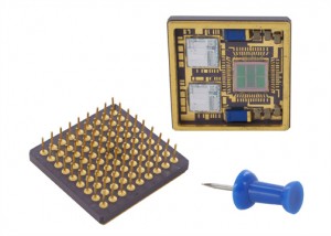
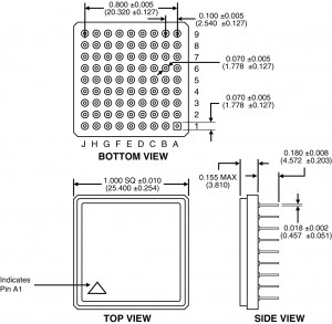
A Pin Grid Array (PGA) is a integrated circuit packaging, where the package is square, with the pins arranged in a regular array on the underside of the package. The pins are commonly spaced 2.54 mm (0.1″) apart, and may or may not cover the entire underside of the package, which are through-hole mounted to a PCB.
| Advantages | Disadvantages |
|---|---|
| Board Space – no extra board space is needed, since the leads are directly underneath the package. | Expense– additional drilling is required to use PGA packages, which makes the boards more expensive to produce. |
| Strength – soldering the PGA via through-hole solder provides a much stronger bond than a surface-mount solder . | Limitations – PGA packages limit the available routing area for signal traces on layers immediately below the top layer on multilayer boards, since the holes must pass through all layers of the to the opposite side. |
| Mounting Options – PGA packages can be mounted to a PCB in two ways. One is through-hole solder. The other is am inexpensive spring-contact sockets. |
QIP
A Quadruple In-Line Package (QIP) is a device package for electronic integrated circuits. QIP packages have the same dimensions as DIP packages, but the leads on the sides are bent into an alternating zigzag configuration so as to fit four lines of solder pads. QIP was developed to increase the spacing between solder pads without increasing package size.
| Advantages | Disadvantages |
|---|---|
| Soldering – the zigzag configuration of solder pads allowed more reliable soldering. | Obsolete – QIP packaging became obsolete in the 1980s. |
| Copper Track – QIP packaging increased the possibilty of running a copper track between 2 solder pads, which is very handy on single sided, single layer PCBs. |
Product Types
Aside from package types, MIL-STD-1553 components have different functionality, which may aid in certain environments.
| Product Type | Package Type | ||||||
|---|---|---|---|---|---|---|---|
|
BGA
|
Flat Pack
|
Gull Wing
|
PGA
|
DIP
|
LPCC
|
QIP
|
|
| Integrated Terminal & Transformer |
X
|
||||||
| Plastic BGA Terminal |
X
|
||||||
| Ceramic Hybrid Terminal |
X
|
X
|
X
|
X
|
|||
| PCI Bridge |
X
|
||||||
| Radiation Tolerant |
X
|
X
|
X
|
X
|
|||
| 1553 Transceivers |
X
|
X
|
X
|
X
|
|||
